Nanoscribe 3D-Lithography
Nanoscribe Photonic Professional GT+
Standard Operating Procedure
Section 1: Process and Experiment Description
Hardware Description
The Nanoscribe 3D Lithography System is a laser lithography system that enables fabrication of true 3-dimensional micro- and nanostructures. Originally designed for the fabrication of photonic crystal structures, the instrument can be utilized for a wide array of 3D structures suitable for applications in different areas of research.
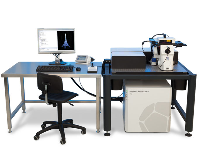
The system utilizes a class 3B (120mW), 780 nm wavelength, 150 femtosecond, 80MHz fiber laser beamed through a microscope objective immersed in a negative-tone photoresist in order to write. The system design utilizes two-photon polymerization (2PP), a technique based on the principle of two-photon absorption, where a molecule absorbs two photons simultaneously to trigger a polymerization reaction. This allows the system to write within a drop of photoresist because the only location with enough energy to polymerize the resist is the voxel formed at the focal point of the objective.
The system utilizes motorized stages in the x,y-plane for scanning across different substrate sizes depending on the substrate holder utilized. The objective approaches the substrate utilizing a z-scanner with a range of around 10mm, and this stage can be utilized for writing tall structures, though with less precision. There are also piezoelectric stages in the x,y, and z-planes, each with a range of 300 um, that can be utilized for greater precision. The z-piezo is utilized for most writes, regardless of the overall size, while the x- and y-piezos (piezo mode) are generally only used for the smallest possible nanostructures. The galvanometer (galvo mode) is used for most writes in the x,y-planes as it is significantly faster than the piezo mode.
Microscope Objectives
There are four objectives available for use with the system for different applications depending on the required feature size, resolution and other parameters used (solution set).
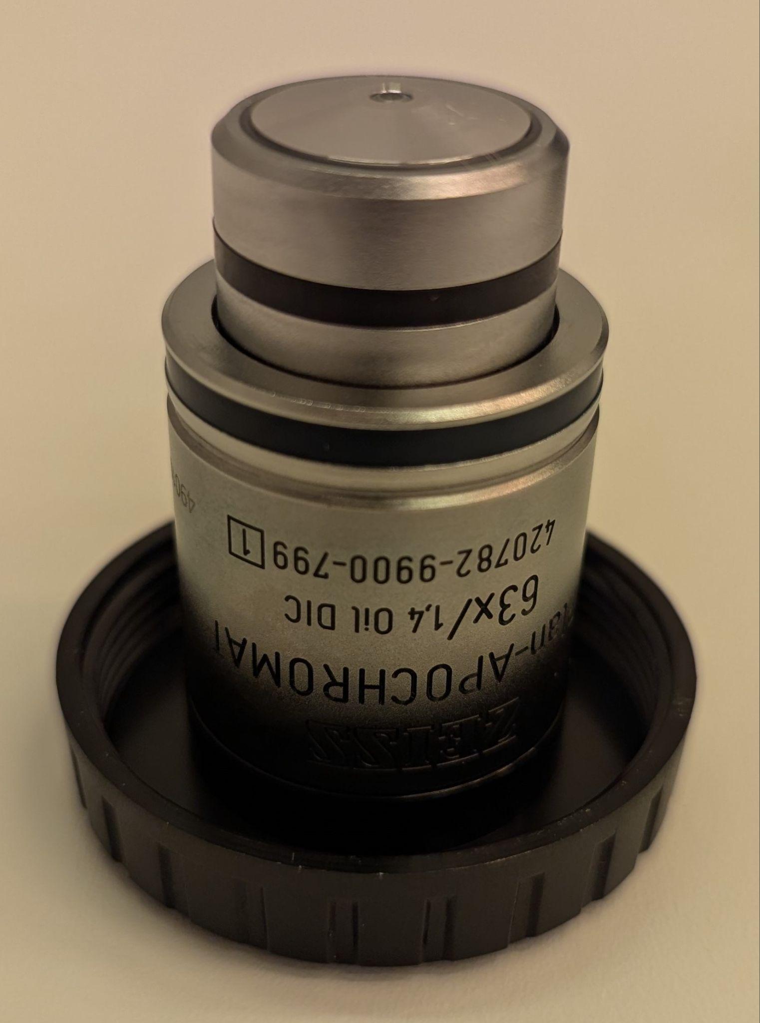
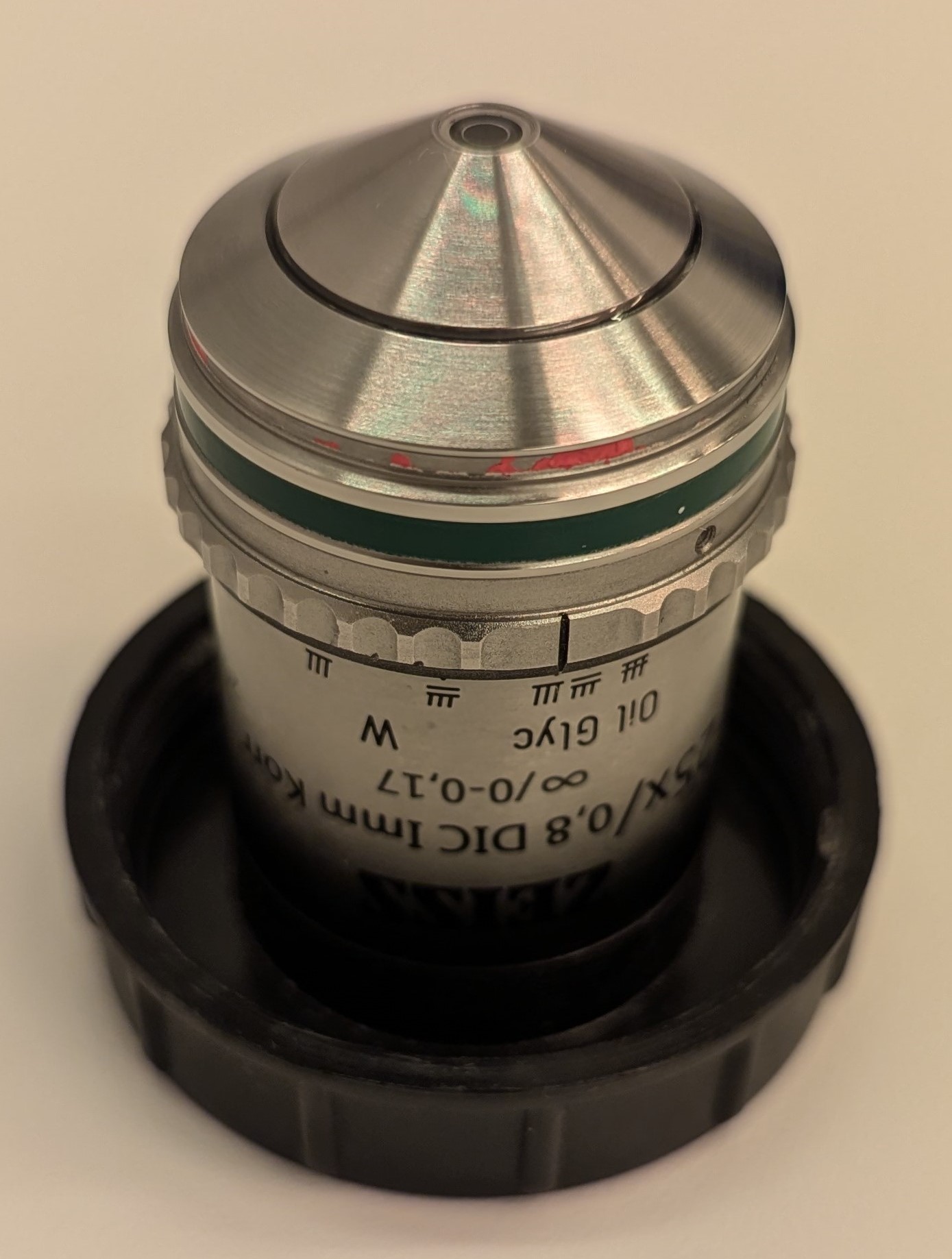
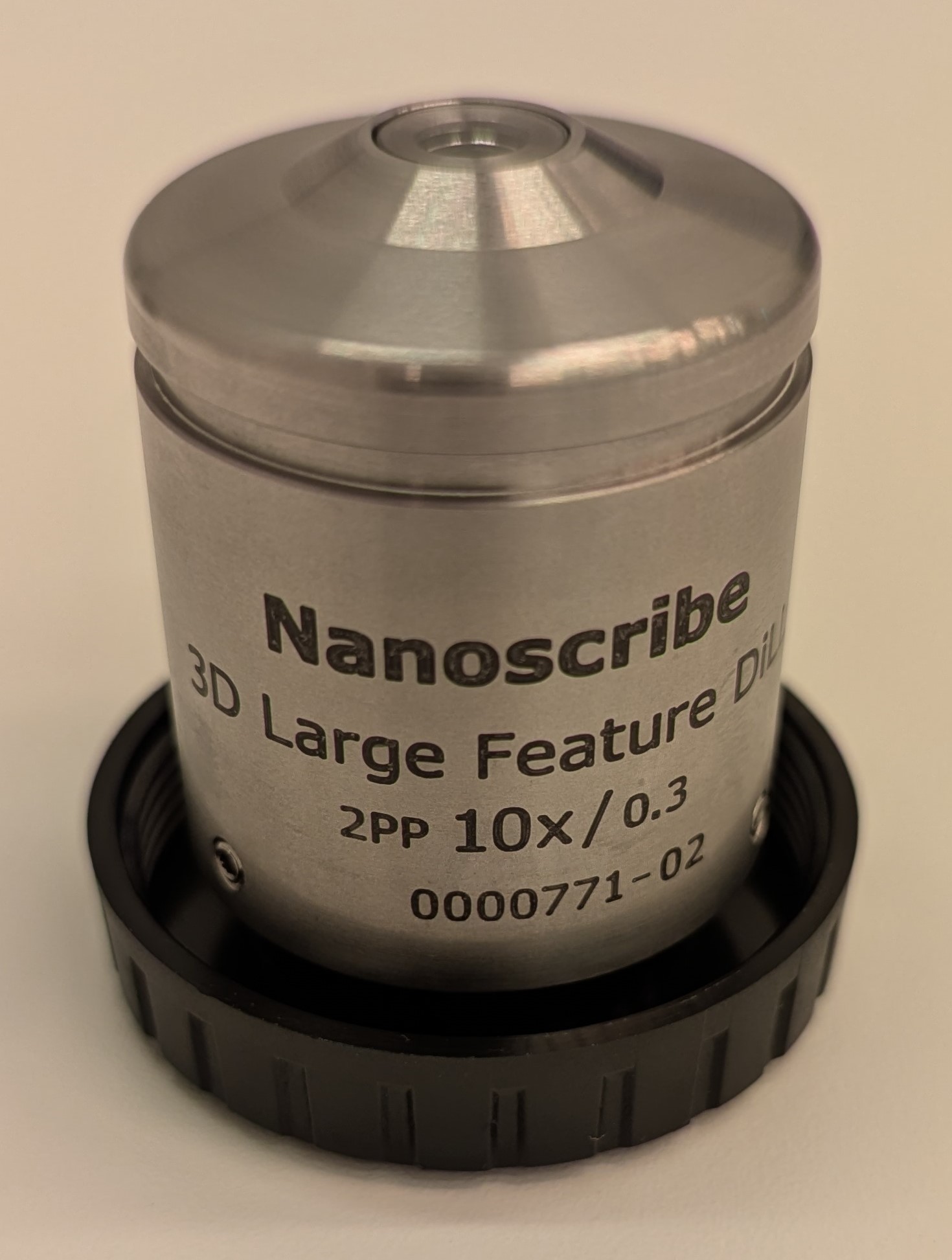
63x NA 1.4: Immersion (DiLL) objective used for small feature solution set (3D SF)
Working distance \= 360 um
Printing field (galvo) \= 200 um diameter circle
Theoretical lateral (x,y) resolution \= 340 nm
Theoretical axial (z) resolution \= 826 nm
Voxel aspect ratio \= 2.4
Δn required at 830 nm \= >0.04
Typical slicing distance \= 0.3 um
Typical hatching distance \= 0.2 um
25x NA 0.8: Immersion (DiLL) objective used for medium feature solution set (3D MF)
Working distance \= 380 um
Printing field (galvo) \= 400 um diameter circle
Theoretical lateral (x,y) resolution \= 595 nm
Theoretical axial (z) resolution \= 3.313 um
Voxel aspect ratio \= 5.6
Δn required at 830 nm \= >0.1
Typical slicing distance \= 1 um
Typical hatching distance \= 0.5 um
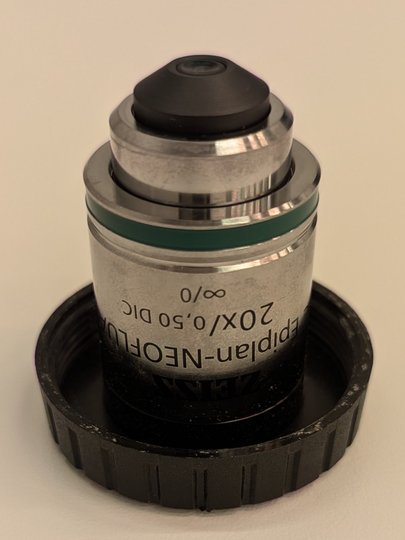
20x NA 0.5: Non-immersion objective used for 2D and 2.5D maskless lithography
Working distance \= 2.1 mm
Printing field (galvo) \= 600 um diameter circle
Theoretical lateral (x,y) resolution \= 951 nm
Theoretical axial (z) resolution \= 5.824 um
Voxel aspect ratio \= 6.1
Δn required at 830 nm \= no limitation
Typical slicing distance \= 3-6 um
Typical hatching distance \= 0.7-1.2 um
10x NA 0.3: Immersion (DiLL) objective used for large feature solution set (3D LF)
Working distance \= 700 um
Printing field (galvo) \= 1 mm diameter circle
Theoretical lateral (x,y) resolution \= 1.6 um
Theoretical axial (z) resolution \= 25.4 um
Voxel aspect ratio \= 16.0
Δn required at 830 nm \= >0.5
Typical slicing distance \= 5 um
Typical hatching distance \= 1 um
Material Description
Nanoscribe GmbH supplies proprietary UV-curable photoresins to be utilized with different applications of the Nanoscribe system. The resins have optimized sensitivity for fast 3D structuring using two-photon absorption with good adhesion to various substrates, low mechanical stress and high mechanical stability. None of the resins require post-exposure bakes. Each resin is optimized to be used with specific objectives, utilizing specific solutions sets to be printed on specific substrates based on the difference in refractive index between the resin and substrate required by the utilized objective.
| 2PP Resin | Refractive Index | Characteristics | Print Set | Objective | Substrate |
|---|---|---|---|---|---|
| IP-Dip | 1.521 | high resolution | 3D SF | 63x | fused silica, silicon, other substrates |
| IP-L | 1.485 | high resolution | 3D SF | 63x | borosilicate, other substrates |
| IP-S | 1.486 | high smoothness; meso-scale | 3D MF | 25x | ITO-coated, silicon, other substrates |
| IP-Visio | 1.486 | low fluorescence; non-cytotoxic | 3D MF | 25x | ITO-coated, superfrost |
| IP-PDMS | 1.43 | highly flexible and elastic; non-cytotoxic; low refractive index | 3D MF | 25x | ITO-coated, superfrost |
| IP-Q | 1.487 | meso-scale | 3D LF | 10x | silicon |
Section 2: Safety Protocols
Potential Hazards
| Hazard | Hazard Sign | Hazard Description | Safety Protocol |
|---|---|---|---|
| Class 3B Laser | 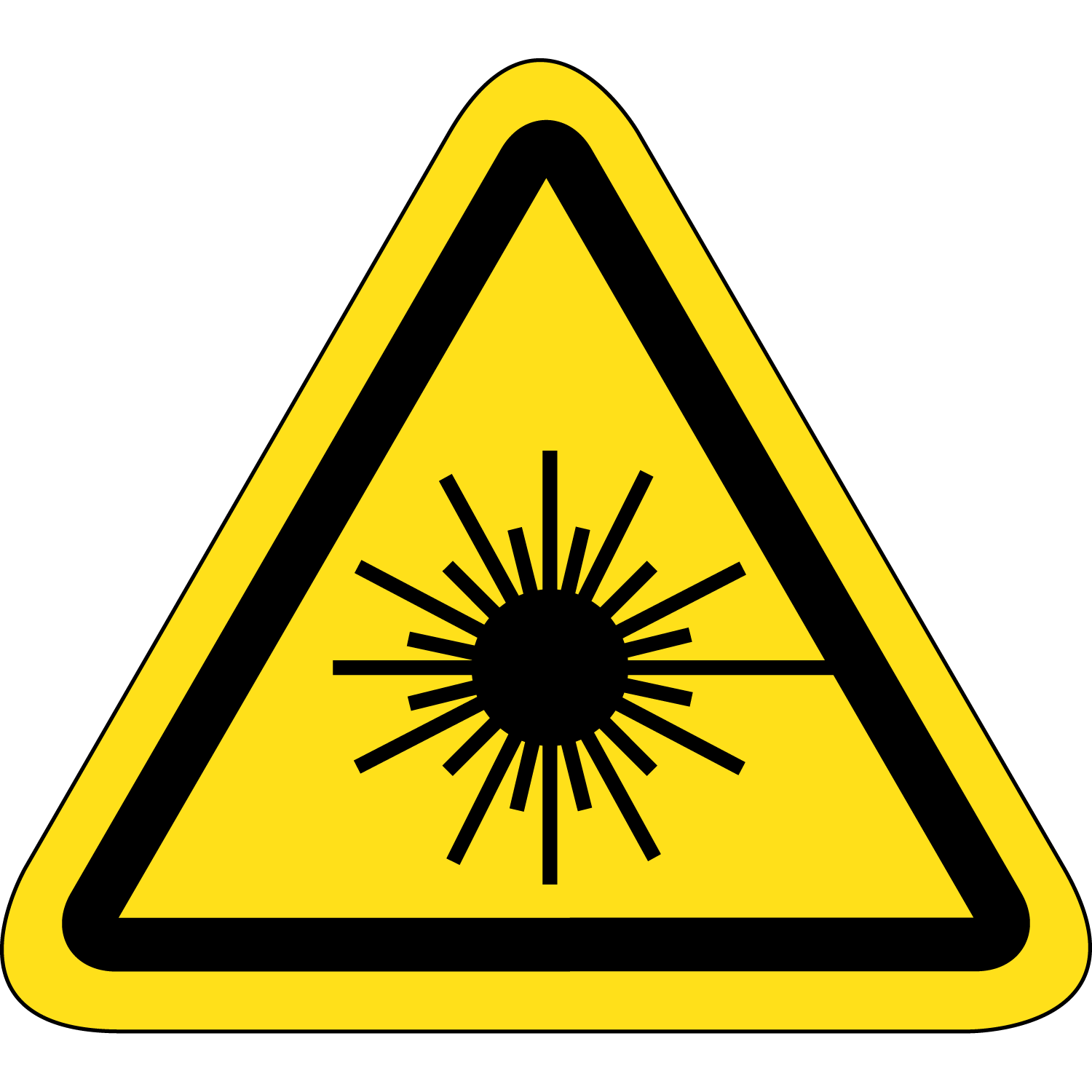 |
Eye hazards: moderate risk level (120mW power) laser may cause immediate eye damage from viewing the direct beam or specular reflections. Skin hazards: prolonged skin exposure can cause burns or skin damage. | Laser shutter is interlocked to close whenever any of the system covers are opened. Users cannot be exposed to the laser when the system is used as directed. |
| Pinch Points | 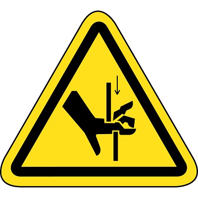 |
Fingers may be trapped between moving parts if placed in the path of moving motorized stages causing minor cuts and bruising. | Stay clear of the motorized stages whenever they are in motion. |
| 2PP Resins [IP-Dip, IP-L, IP-S, IP-Visio, IP-PDMS, IP-Q] |  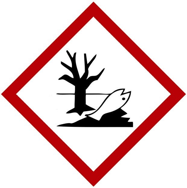 |
Causes serious eye irritation. Causes skin irritation. May cause an allergic skin reaction. Toxic to aquatic life with long lasting effects. | Users are required to wear cleanroom gloves and safety glasses at all times in the cleanroom. It is also recommended to wear a second pair of nitrile gloves whenever handling photoresins. Change gloves whenever gloves are soiled by photoresin. Dispose of soiled gloves in a red garbage bin. |
Personal Protective Equipment Requirements
Users must be wearing the nitrile cleanroom gloves and safety glasses required throughout the cleanroom whenever using the Nanoscribe. No extra personal protective equipment is required.
Waste Disposal
Dispose of gloves and wipes soiled with photoresin or solvents in a red hazardous waste bin.
Dispose of used or failed substrates in a sharps waste container.
Section 3: Process Procedures
Estimated Time: \~40 minutes + write time
Material Requirements
Equipment: substrate, tweezers, three glass containers (for Surpass [optional], PEGMA developer and IPA), tape and vertical substrate holder
Start Up Tool
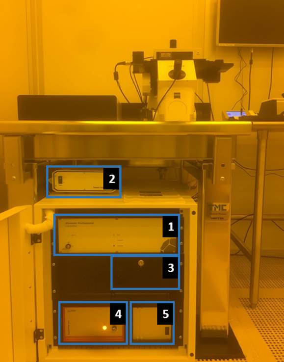
- Turn on the controller
- Turn on the power supply
- Turn on the computer
- Turn on the laser
- Turn on the motorized stages
- Log onto the computer as “User” with password “Hilda001”
- Confirm that the objective you intend to use is selected in the microscope controller.

Initialize Software
1. Click NanoWrite software icon on the desktop.
2. Click Calibrate in the "Stage calibration" window that pops up.
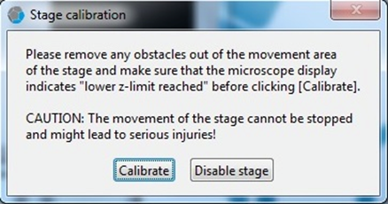
3. Wait until the calibration process is done.
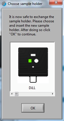
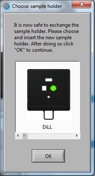
4. The "Choose sample holder" window appears when the calibration process is done. It is ready to load the sample.
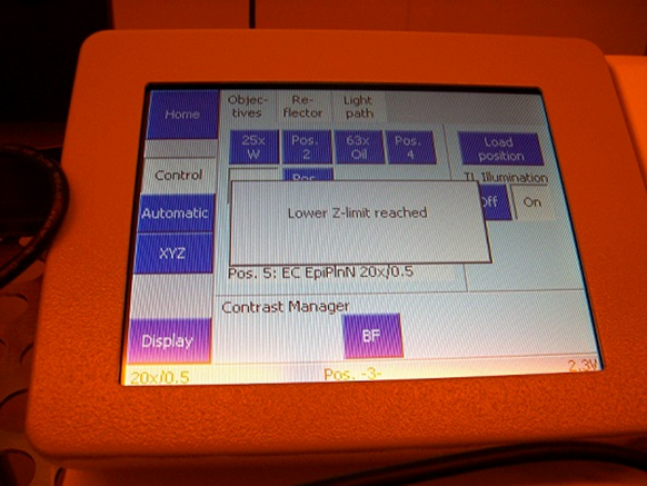
5. Confirm on the microscope controller that the objective turret (Z-stage) is in the lowest position.
Sample preparation
1. Choose the sample holder.
2. Clean the substrate.
a. Here is the cleaning procedure in the user manual (Chapter 5.3 of User_Manual in Nanobox file directory on the PC):
                                              i.    Rinse the substrate surfaces with acetone.

                                             ii.    Rinse the substrate surfaces with IPA.

                                            iii.    Rinse the substrate surfaces with distilled water.

                                           iv.  Blow-dry the substrate with nitrogen.
Notes:
· Using this cleaning method, a droplet of resist will not spread strongly over the substrate surface. Alternative cleaning methods (e.g. oxygen plasma) might change the wetting properties of the substrate surface so that the droplet will cover a bigger area, which may be desirable in some cases.
· IPA can be replaced by methanol in the above cleaning method.
3. Fix the substrate on the sample holder with tape.
4. Put a drop of oil or/and resist on the substrate carefully. The following example is immersion configuration: resist on the bottom side.
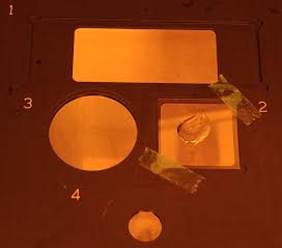
5. Insert the sample holder into the microscope module. Make sure that the sample holder is set at the right position. When the sample holder is inserted, you can hear a "click sound".
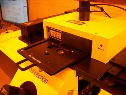
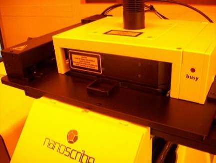
Note: There are the following three printing configurations (see Chapter 5.2 of User_Manual in Nanobox file directory on the PC).
a. Oil immersion configuration
b. Air configuration
c. Dip-in laser lithography (DiLL)
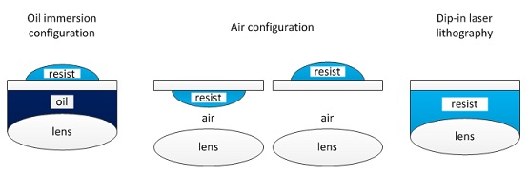
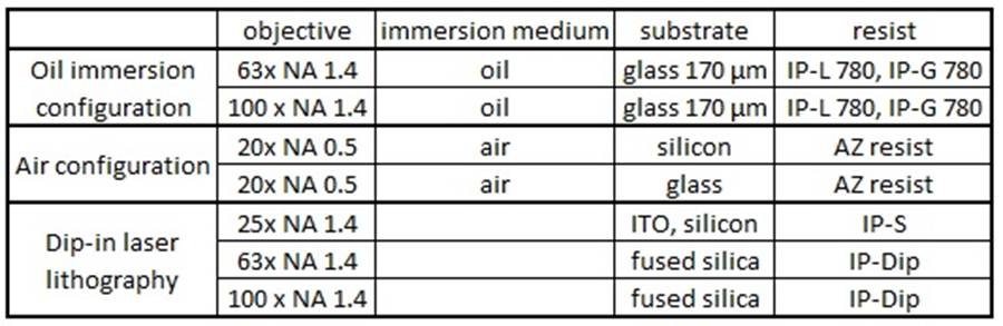
Note: Resolution depends on the objective lens and resist.
Install Objective Lens [Additional Training Needed]
1. Press the objective lens button on the microscope controller for the replacement position.
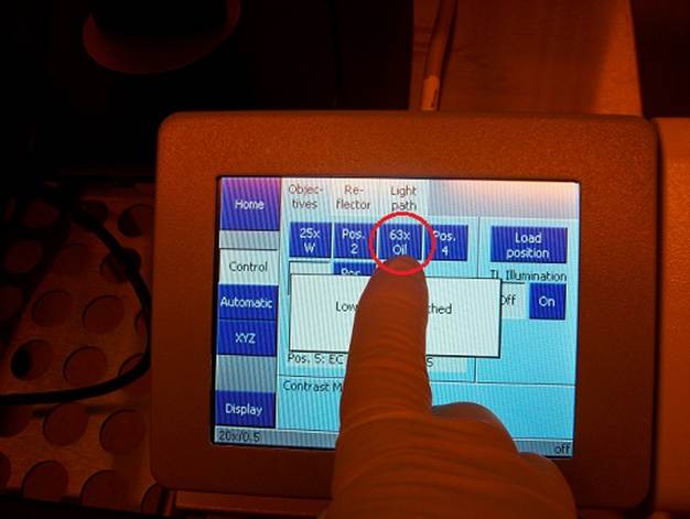
a. For example, if you want to use 63x objective lens, press the 20x button, and the #3 pocket for the 63x objective will rotate to the right side of the module.
2. Remove the cap from the pocket of the turret if it is present.
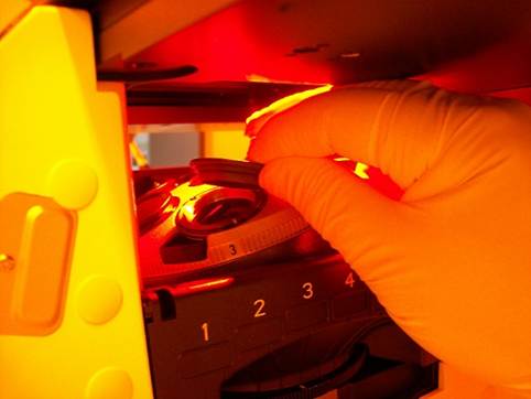
3. Remove the objective lens from the case. A white suction ring must be put on the objective lens.
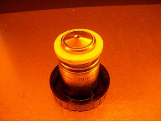
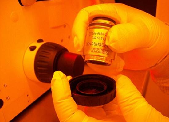
4. Install the objective lens on the objective turret of the microscope module.
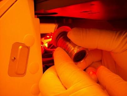
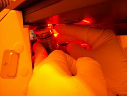
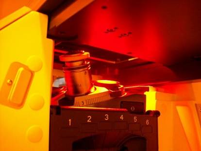
5. On the Zeiss touch screen, press the button of the objective lens installed, and the objective lens will move beneath the sample.
3D Writing Procedure
1. If you haven’t done so already, click on the sample location in the "Choose sample holder" window, and the location clicked will be in green.
2. Click the OK button.
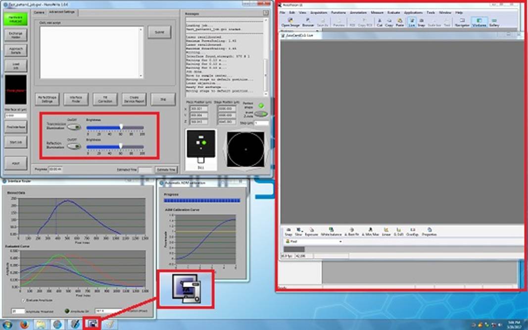
3. Click the  icon on the bottom of the screen, and the monitor window and illumination LED switches will be opened.
4. Click on the button of the transmission or reflection illumination.
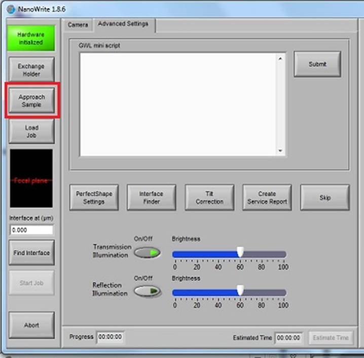
5. Click the Approach Sample button.
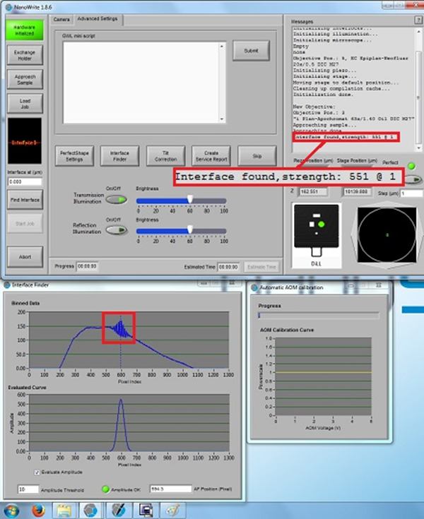
6. When the right working distance is automatically found, the small interference fringes will be observed in the "Interface Finder" window, as shown below. If the small interference fringes are not observed, or located at the wrong pixel, you have to click Find Interface later.
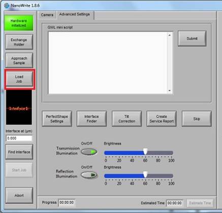
7. Click Load Job, and the "Open File" directory will be opened.
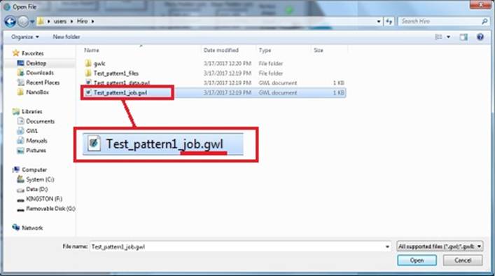
8. Open the xxx_job.gwl file.
9\. Click **Start Job**.
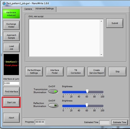
a. Note: If the interface is not found in the process of "Approach Sample", you must click Find Interface before starting job. Then, make sure that the small interference fringes are seen in the "Interface Finder" window.
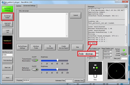
10. After the job is done, click the "Exchange Holder" button.
Unload Sample
1. Click the OK button in the "Confirm exchange holder" window.
2. Remove the sample holder from the microscope module.
3. Remove the sample from the sample holder.
4. Turn off the illumination LED, if necessary.
Develop Sample
1. Use a bath of SU-8 developer (propylene glycol monomethyl ether acetate, PGMEA) in a 25 mL beaker. To fix the substrate vertically in the beaker, use the vertical substrate holder. Allow the substrate to develop for at least 10 minutes. Depending on the size of the structure, this step can take up to 30 minutes. However, the development time is not very critical – structures can be kept in the developer for much longer without changing the structure.
2. When development is done, carefully remove the holder from the PEGMEA and place into a second beaker containing IPA for 1-2 minutes. Do this carefully – the surface tension of the liquids can easily destroy fragile features.
3. Remove from the IPA and place the substrate on a clean surface to air dry. For more robust structures, methanol can be applied to the surface to expedite evaporation. DO NOT blow dry the substrate.
Shut Down Tool
1. Turn off software and shut down the computer.
2. Turn off stage.
3. Turn off laser.
4. Turn off microscope.
5. Turn off microscope power.
6. Turn off main power.
Cleanup and Waste Disposal
1. Check tool for any residual resist and clean with wipes and IPA.
2. Dispose of used developer in the correct SU-8 Developer (PEGMEA) bottle kept in the lithography bay waste cabinet across from the Nanoscribe system, under the table.
3. Rinse, dry and put away all glassware and tools used.
4. NanoFab Staff will routinely clean the objectives.
Emergency Stop
- NA
What to watch out for during operation
- Laser not firing.
- Interface not found during approach.
- Stage not initializing after the tool is turned on.
Allowed Activities
- Users may use substrate/holder combinations according to the following parameters:
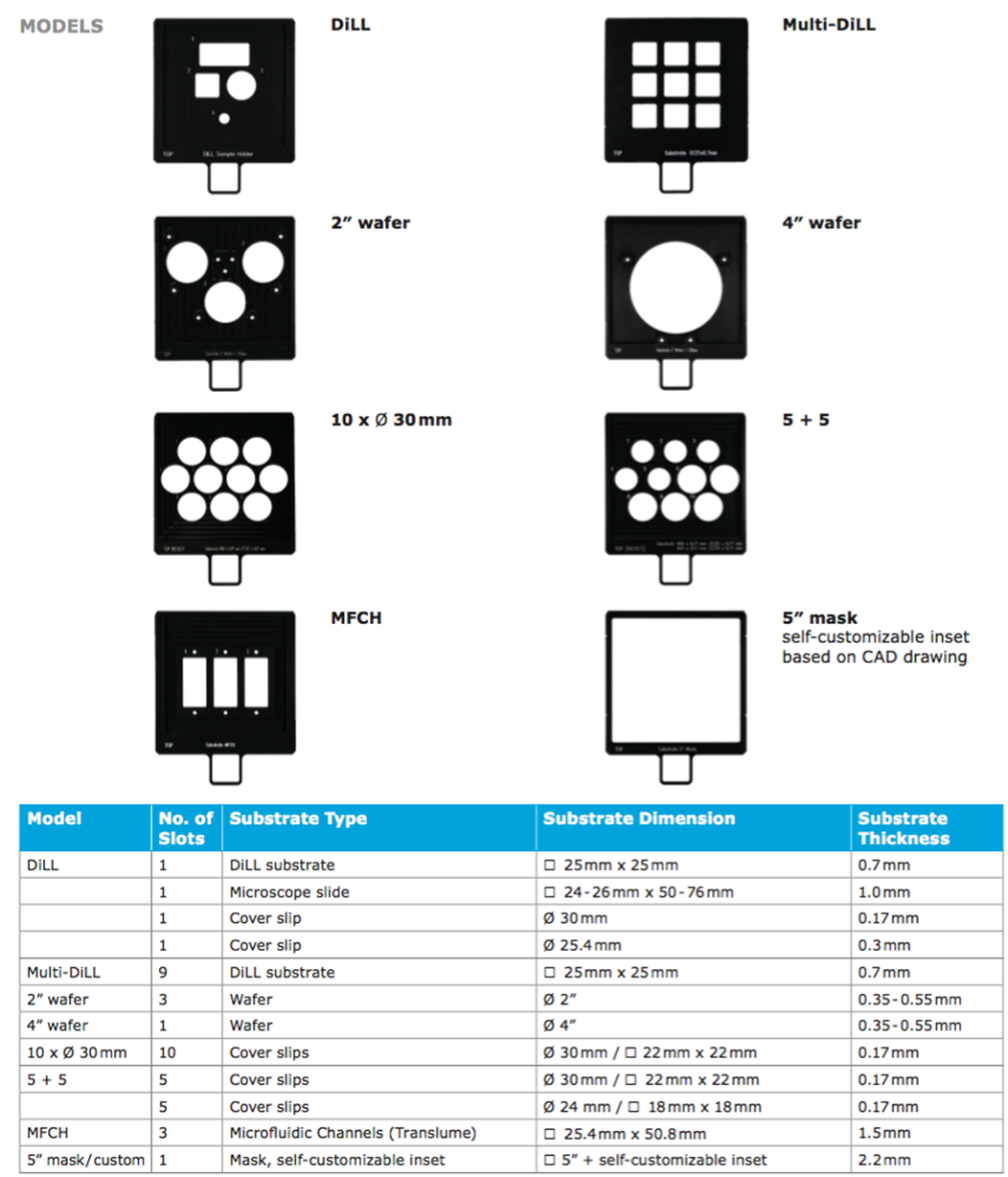
- You must have permission from staff if you wish to use a holder/substrate combo different from this, which requires special training on finding the interface.
- Users are allowed to use non-Nanoscribe resists with NanoFab Staff permission and only in a non-dip-in mode.
Disallowed Activities
- Don’t remove the sample holder unless the exchange holder window has been selected and the window is open.
- Don’t crash the objective into the substrate.
- Don’t use a resist that isn’t already on the objective that you are using.
- Don’t try to clean the objective unless you have been trained to do so.
- Use non-Nanoscribe DIP resists in dip-in (DiLL) mode.
Common Troubleshooting Tips
- If the previous user did not shut down the system in the instructed order, the tool will sometimes have issues finding the interface. If this is the case, shut down the tool in the instructed sequence and then restart from the beginning.
- If you continue to have issues finding the interface, schedule a meeting with NanoFab staff. The Nanoscribe interface finder is highly dependent on the substrate thickness, sample holder position used and index contrast at the interface. NanoFab staff can advise the best course of action if you are using a non-standard substrate.
- If you write, develop and inspect, to find nothing on your substrate, consult the NanoFab staff. Common issues are:
- Adhesion issues, which can be improved with surface modification techniques, such as 02 plasma exposure, 02 ozone exposure, or adhesion promoters.
- STL design issues, which can be improved by adjusting writing parameters (hatching and slicing) in the setup process of your run files.
- Writing power and scan speed issues, which can be adjusted to optimize exposure dose for a particular design.
When to call staff?
- If the tool will not initialize.
- If the tool does not find the interface.
- If the objective crashes into the substrate at any point.
Badger Criteria
Report Problem
- Visible debris on the objectives (objectives need cleaning).
Shutdown
- Tool will not initialize.
- Tool will not power up.
- No laser power reported during interface finding.